The VME-TEM2 is the readout module for the GLAST tracker. It has been used for the BTEM testbeam (1999) and lab testing. It has been developed and build by Stanford University.
The following table shows the VME addressing of the TEM. The base address is set by dip switches on the board. The default address that are used are 0x8000000 and 0x4000000.
| address | A32 |
| base address | 0x8000000 or 0x4000000 |
| address range | 0xffff (??) |
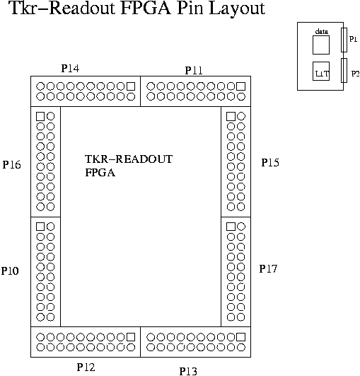
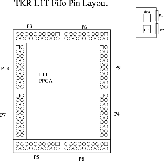
The following table shows the pins to monitor the command, token and data for the eight cables. In the table PN, M means pin M on connector PN (a connector has 20 pins). The connectors are for the Data FPGA (P10-P17) and the L1T FPGA (P3-P9,P18).
| cable Nr. | command | data | token |
|---|---|---|---|
| 0 | P11, 2 | P17, 19 | P10, 16 |
| 1 | P10, 5 | P17, 16 | P12, 11 |
| 2 | P15, 13 | P15, 12 | P16, 11 |
| 3 | P15, 16 | P10, 9 | P16, 15 |
| 4 | P15, 15 | P10, 20 | P16, 16 |
| 5 | P14, 11 | P10, 17 | P11, 4 |
| 6 | P12, 12 | P17, 17 | P10, 19 |
| 7 | P14, 12 | P16, 7 | P14, 10 |
There is one trigger acknowledge, (P14, 13), that is send to all cables. The clock is found on pin P7, 1 (L1T FPGA).
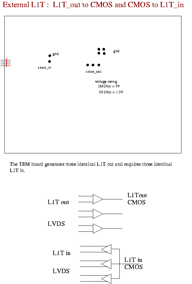
The L1T is the main trigger that trigger the readout sequence for the trigger. A L1T is generate in multiple ways.
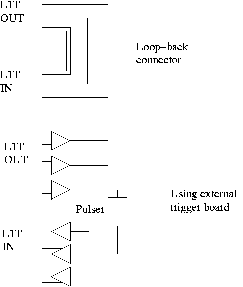
If the TEM board is used in stand alone mode the L1T out and the L1T in have to be connected using the loop-back connector which just connects the input and output. Actully there are three input and output lines. The three input lines are connected to a logic AND to reduce the noise sensitivity.
Instead of using the simple loop-back connector a trigger board was build. The L1T out signal are converted to CMOS signals. One of these signals is used to trigger a pulser which generates the incoming the L1T in, which is converted to three lvds signals as input to the TEM. The external trigger board. The figure shows the two different configurations.