The sensitivity of the AToM chip to the clock duty cycle was measured for radhard chips before and after irradiation (1Mrad). The measurements were performed at 16 ns (62.5 MHz) clock period.
We measured the sensitivity to the clock duty cycle. The write register command is most sensitive to the clock duty cycle: 51 % - 61 % (radhard, no Irr.) and increases after irradiation: 57 % - 60 % (radhard, 1Mrad Irr.).
The command decoding, read register, token passing are working fine in a much wider range (for details see further below). After the irradiation the duty cycles ranges gets smaller in particular at the lower edge.
The lower value off the duty cycle depends on vdd: -0.025 %/mV.
All measurements were performed at 16 ns clock (62.5 MHz). Four different command sequences were send to the chips:
The Sequences 1 and 2 contain writing of the individual register which is the most sensitive action in respect to the duty cycle sensitivity. The duty cycle was measured at the input of the chip (CLK+ - CLK-) using the width at the 50% point.
The measurements were performed using:
Command Decoding: The interpretation of the commands functions over a wide range of duty cycles. Sending just a Read Register command (s2) works within a range of:
Token passing: The token passing was also working in a wide range if only a Trigger Accept and Read Event command were used (s4). If writing shift registers were used (s3) it was working only in a very limited range.
Write Register: The most critical part is the writing of the register: Using the command sequence s1 the following symptoms were observed: The following list shows the symptoms observed (duty cycles values are for non irradiated radhard chips):
The following values were measured for the range the write register works fine:
| board 6, no irradiation |
board5, after irr. 1 Mrad |
board 5, before irradiation |
|
51.4 - 63.0 (chip 11) |
57.0 - 60.5 (chip 11) | 53.5 - 63.2 (chip 11) |
| 51.2 - 62.2 (chip 2) | 54.0 - 61.3 (chip 2) | 51.5 - 63.2 (chip 2) |
|
49.5 - 61.5 (chip 1) |
55.2 - 61.2 (chip 1) |
52.0 - 62.1 (chip 1) |
The statistic is still very limited: 6 radhard chips before irradiation
and 3 chips after irradiation. The lower value of the duty cycle range
varies more than the upper value. The results (writing the register) are
shown in the previous table.
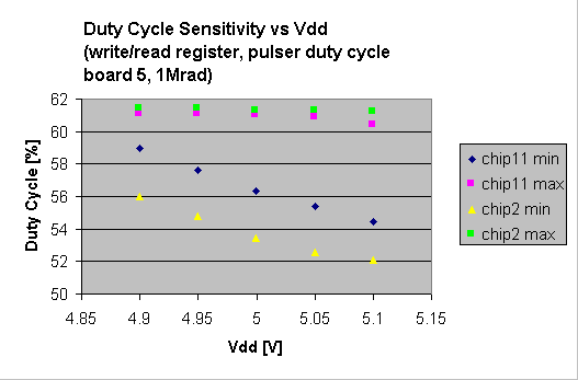
For the command sequence: reset, write reg. and read reg. the duty cycle range was measured for different Vdd values. This measurement was done for board 5 after irradiation. The following figures shows the results for two different chips. The slope of the minimum duty cycle is about 0.025 %/mV. There is also the big difference in the offset between chip 11 and 2.
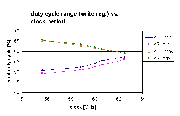
The workable duty cycle range for the write register command depends strongly on the clock period as shown in the following figure. The measurements were done for irradiated radhard chips.